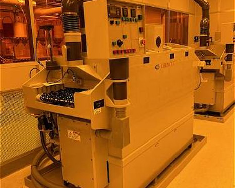
Chemcut Differential Copper Etch System
This Chemcut tool is ideal for researchers needing to use differential etching of a copper seed layer. It can take up to 16” panels and has oscillating nozzles on both sides to spray uniformly. It can etch silicon, organic, and glass substrates.
The Chemcut is able to yield a 3:1 differential etch using a dual-etching process that can remove copper while allowing for detailed patterns and designs to remain in the underlying substrate. This system operates at low temperatures to reduce the thermal stress on substrates and achieve better uniformity. The capabilities of this system make it ideal for achieving high levels of detail with controlled production quality.
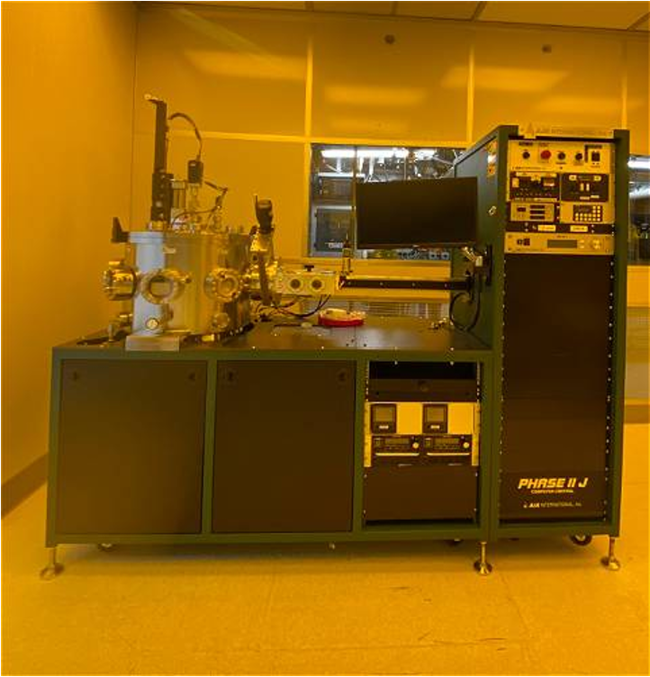
AJA Chalcogenide Sputterer
This AJA tool is ideal for researchers needing to deposit chalcogenide materials in a nitrogen enriched low vacuum. It has both an RF and DC power supply with two switch boxes that can switch between 9 different materials. Some of the materials include: Ge2sb2Te5, Ge2Sb2Se4Te1, GeTe, Sb2S3, and ITO.
This AJA is known for its high reliability and advanced capabilities in sputtering technology. The AJA even has an RF Bias power supply that can reach up to 800C which may be helpful for preheating substrates. The variety of capabilities this system has makes it ideal for producing high-quality chalcogenide films with controlled thickness and composition
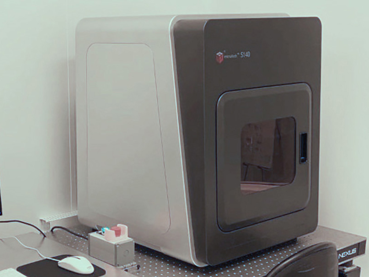
Boston Micro Fabrication s140 3D Printer
The BMF microArch S140 is the ideal solution for researchers requiring ultra-high resolution, accuracy, and precision in a desktop micro 3D printer. The microArch has a large build volume (94x52x45mm) and the ability to print with engineering-grade materials (photosensitive resins) to meet the needs of industrial production and quality. With an optical resolution of 10μm and layer thickness of 10-40μm, the S140 can produce surface finishes of 0.4 - 0.8μm Ra (top) and 1.5 - 2.5μm Ra (side).
BMF microArch is the first commercialized high-resolution, 3D microfabrication equipment based on PμSL technology. Projection Micro Stereolithography allows for rapid photopolymerization of a layer of liquid polyer using a flash of UV-LED at micro-scale resolution.
Experience the fast and easy production of microstructures by importing your STL file and exposing your design directly to accelerate your work in the areas of microfluidics, MEMS, filtration, electronics, medical devices, and other applications that require microstructures.
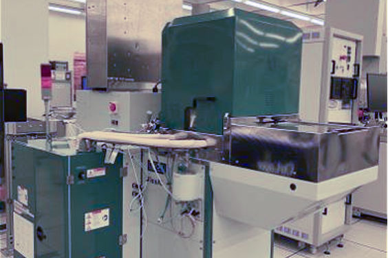
Oxford FlexAL ALD
This popular tool is capable of plasma ALD and thermal ALD processes within a single process chamber. The Oxford FlexAL ALD is designed to grow layer-by-layer thin films while ensuring precise control, film conformity, and film repeatability. It uses heated precursors to deposit various metals along with gases for plasma-assisted oxides and nitrides.
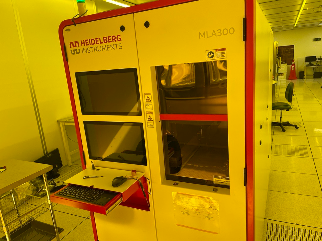
Heidelberg MLA 300
This maskless lithography system is designed for easy operation to develop photoresist films. The Heidelberg MLA streamlines prototyping cycles and achieves the highest optical quality and precision. It uses a light to expose many types of photoresists including thicker and harder to reach layers.
The Maskless Aligner MLA 300 provides high throughput, a simplified workflow, and integration with manufacturing execution systems. With a minimum feature size of 1.5 um, the MLA 300 can expose up to 12" wafer sizes. Real-time autofocus compensates for substrate warp or corrugations, ensuring flawless patterning. Utilizing this tool, researchers will spend less time writing circuit patterns, thus shortening the lag between prototyping and production while maintaining superior critical dimension (CD) uniformity.
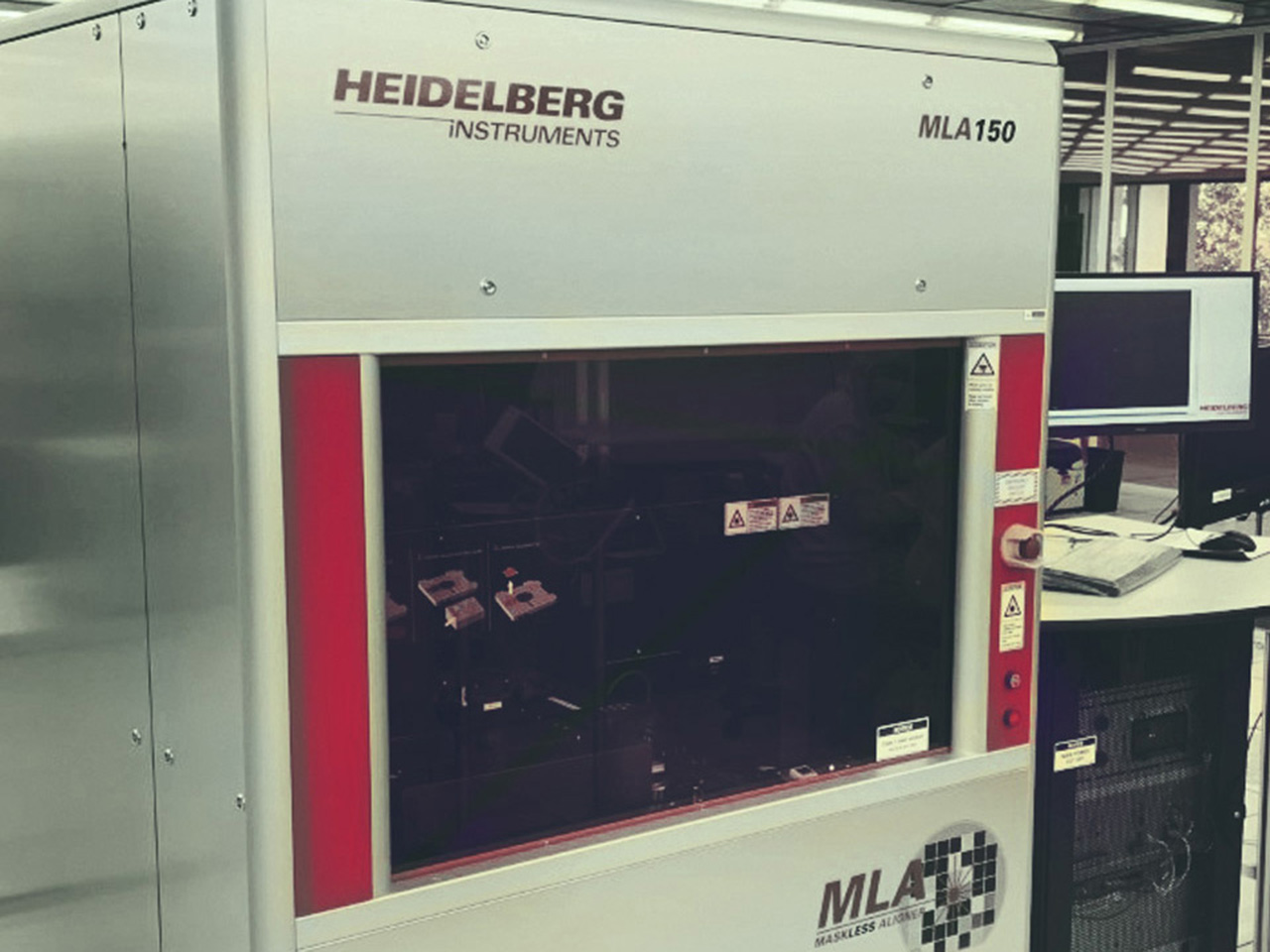
Heidelberg MLA 150 #2
The Heidelberg MLA 150 #2, located in the Marcus Inorganic cleanroom. This maskless lithography system is designed for easy operation to directly develop photoresist films. The Heidelberg MLA streamlines prototyping cycles by allowing patterns to be exposed directly and offers topside alignment. It uses a light to expose many types of photoresists including thicker and harder to reach layers.
The MLA 150 #2 stands out due to its high exposure speed, accommodates any size and shape, and has flexible pattern changes. It can expose an area of 100 x 100mm2 with structures as small as 0.6um and an alignment accuracy of 500nm between layers. This tool can support two wavelengths of 375nm and 405nm, a substrate minimum size of 1.5cm x 1.5cm and perform topside alignment. We hope this tool will greatly aid researchers who are working in the areas of Life Science, MEMS, Micro-Optics, Semiconductor, and other applications.
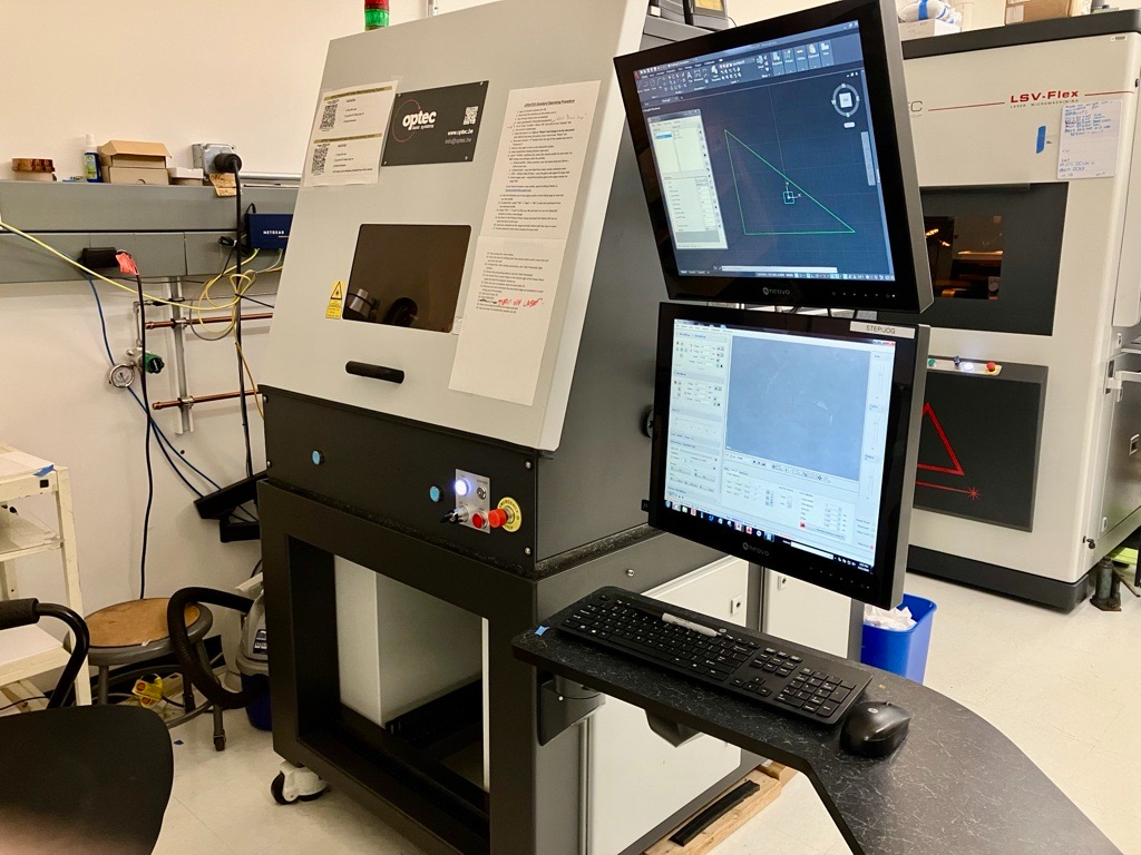
Optec Femtosecond Laser
The Georgia Tech Optec Femtosecond Laser is an OPTEC WS-Flex USP system that uses a femtosecond laser to process practically any material through ultra-short laser pulses photo-ablation. The ultra-short laser pulse is effective on polymers, metals, ceramics, glass, single crystals, and polymorphic crystals. Materials are ionized by the laser pulse and removed from the surface in a plasma cloud, leaving a clean surface at the interaction site. Contrary to typical thermal laser operations, the femtosecond laser is not as sensitive to wavelength absorption and creates minimal thermal gradients, therefore leaving no heat-affected zones on processed materials.
Applications include cutting, milling, drilling, tube processing, composite material cutting, scribing, and surface structuring.
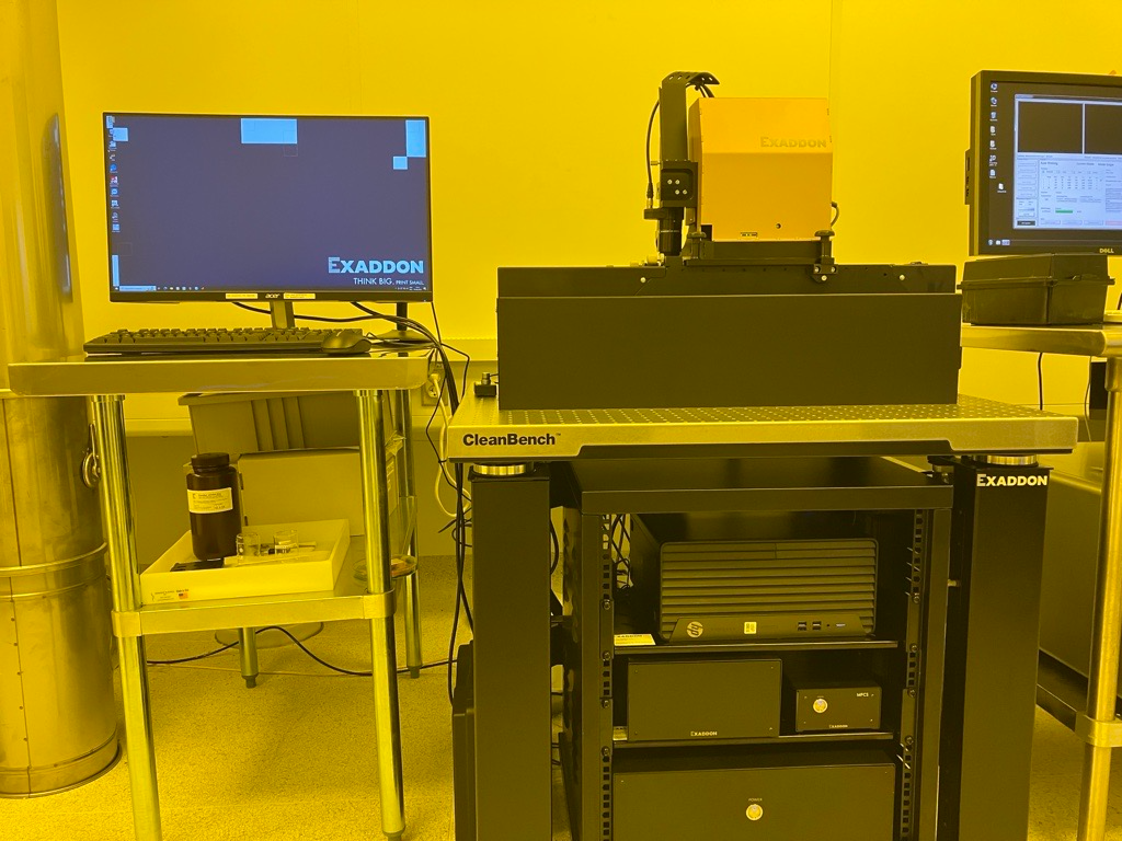
Exaddon CERES μAM
The Exaddon CERES μAM system prints microscale metal objects by electrodeposition. The system is optimized for printing free-standing microscale structures such as pillars, needles, coils, and lattices on existing surfaces, such as ICs or wafers.
Printing occurs at room temperature, and no post-processing is necessary. This system can print Gold, Copper, and Nickel. The printable size range is 1 μm – 1 mm, resolution < 1 μm, and structures can be located on print surfaces with <1 μm accuracy. This makes it ideal for applications in brain-machine interfaces, semiconductor surface modification, Photonics, Drug Delivery, and HF communication components.
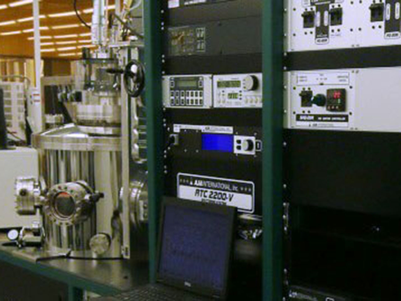
AJA Nitride Multisource Sputtering System
The Georgia Tech AJA Nitride Multisource Sputtering System deposits thin metal and nitride films in argon and nitrogen-enriched low vacuum. The AJA Sputterer has 4 magnetron sputtering guns, 2 DC power sources, 3 RF power sources, and a heater that can reach up to 800°C. It also has the capability of pulse dc. RF Bias is also available up to 50W. It can process wafers up to 4" -Deposition Processes: Aluminum, Aluminum Nitride, Titanium, Titanium Nitride, W, Mo, Ta, and Tantalum Nitride.
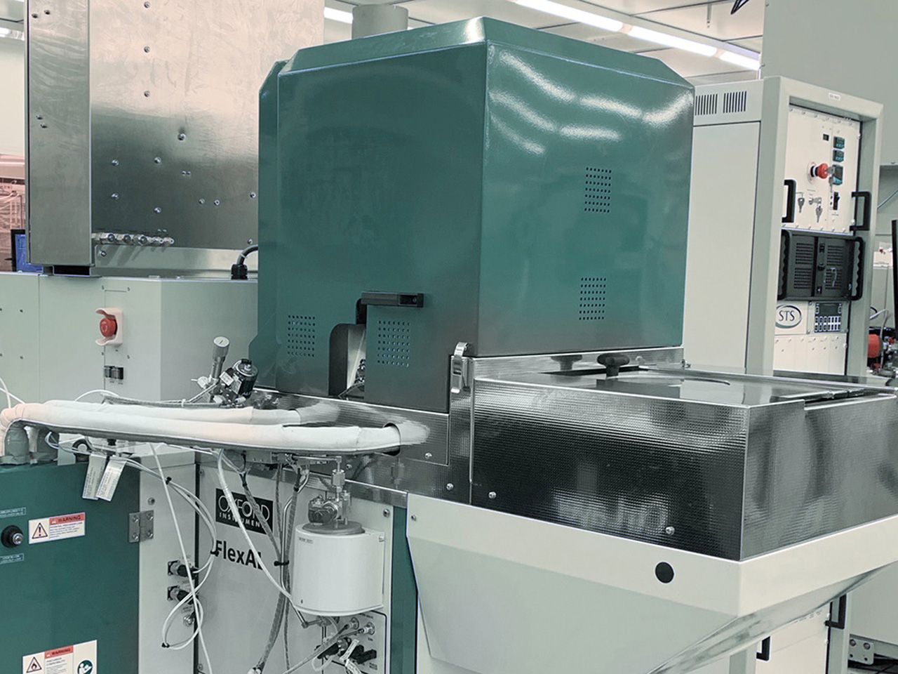
FlexAL Atomic Layer Deposition System
The FlexAL atomic layer deposition (ALD) system offers a broad range of optimized high-quality plasma ALD and thermal ALD processes with maximum flexibility in precursors, processes gases, and hardware configuration within a single process chamber.
Features include:
- Remote plasma for low damage plasma ALD combined with thermal ALD in one deposition chamber
- RF biased electrode option available for control of film properties
- Industry-standard cassette to cassette handling for higher throughput
- Maximum flexibility in the choice of precursors, process gases, hardware features and options
- Optimized to maintain low-damage, high-quality substrates
- Removable liners allow for easy chamber maintenance
- Low temperature to enable high-quality deposition on temperature-sensitive surfaces